Peculiar quantum-nano structure formation in GaAsBi nanowires triggered by atomic crystalline defects
We are investigating the crystal structure of GaAs/GaAsBi/GaAs core-multi-shell heterostructure nanowires, which have potential as materials for next-generation nanoscale communication band lasers, quantum light sources, and solar cells. These nanowires are made of semiconductor crystals. There are twin defects in the material where the atomic arrangement is switched in the mono-atomic layer. This induces a peculiar structural deformation and a characteristic quantum nanostructure formation.
Semiconductor nanowires are attracting attention as a potential material for next-generation ultra-small electronic devices. Epitaxial growth that assembles crystals at the atomic level enables the integration of compound semiconductor nanowires with superior electronic and optical properties on the developed Si platform. The GaAs material, conventionally used for communication lasers, optical amplifiers, sensors, etc., suffer from inherent Auger recombination, which induces heat generation during the conversion between electrons and light. To avoid this, the dilute bismuth material, GaAsBi, has been attracting attention in recent years. The Ehime University group has succeeded in using GaAsBi semiconductors as nanowires. In addition, from high-precision crystal growth, while maintaining a good crystal structure, a GaAs core forms inside the needle-shaped nanowires, and GaAsBi and GaAs are layered around it. This multi-layered structure can be used as the basic structure of lasers, LEDs, and solar cells.
We reported our investigation of the detailed crystal structure of GaAs/GaAsBi/GaAs core-multishell heterostructure nanowires. Some have twin defects, in which the atomic arrangement is switched at the mono-atomic layer. In particular, we found a unique structural deformation induced by the presence of this twin and a specific segregation of Bi elements at that site. It is known that electrons and light can be confined to the area where Bi accumulates. We thus reported the possibility that the characteristic nanoscale structure formed here could be an unprecedented quantum nano material.
Bibliographic Information
Twin defect-triggered deformations and Bi segregation in GaAs/GaAsBi core–multishell nanowires, Teruyoshi Matsuda, Kyohei Takada, Kohsuke Yano, Satoshi Shimomura, Yumiko Shimizu, Fumitaro Ishikawa, Appl. Phys. Lett. 117, 113105, doi: 10.1063/5.001309, 2020 (September 18).
Fundings
- Japan Society for the Promotion of Science(JSPS) KAKENHI Grant Numbers JP19H00855 and JP16H05970
Media
-
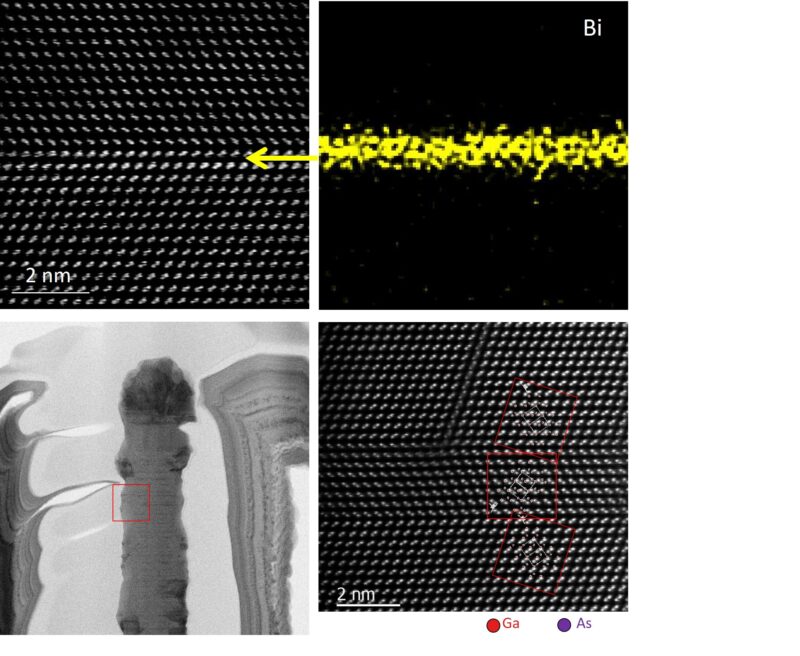
Electron microscopy for a GaAsBi nanowire
Atomic arrangement and distribution of Bi elements in a nanowire. Appearance with rough deformation on the surface and crystal structure inside. At the site where the crystal arrangement is switched, the crystal structure is greatly deformed on the surface. In addition, Bi aggregates locally in almost one atomic layer to form a characteristic quantum/nanostructure.
credit : Ehime University
Usage Restriction : Please get copyright permission
Contact Person
Name : Fumitaro Ishikawa
Phone : +81-89-927-9765
E-mail : ishikawa.fumitaro.zc@ehime-u.ac.jp
Affiliation : Graduate School of Science and Engineering